RT4803B Product Overview:
High-Efficiency Boost Converter with Integrated Bypass Switch and 1.2V I/O Support
Sion Lin, Chad Chen, Sophia Tong | AN086
Richtek has launched the RT4803B, a low-voltage synchronous Boost converter specifically designed for Li-Ion battery-powered applications. It features an integrated bypass switch (BYP_FET) to enhance system efficiency and flexibility, ensuring stable operation.
In boost mode, the RT4803B supports output currents up to 3A. With a shutdown current of less than 1μA, it extends battery standby time, making it ideal for long-idle standby applications.
A key feature of this Boost converter is it supports I2C communication with a 1.2V I/O interface, addressing the requirements of future low-voltage digital devices in advanced process technologies. It provides a high-performance, low-power solution suitable for powering components such as 2G PAs, Wi-Fi modules, and audio amplifiers in Li-Ion battery-powered devices.
1 Product Topology: Key Advantages
of the Integrated Bypass Switch
Integrated with the bypass switch, the RT4803B provides three distinct advantages over conventional boost converters.
1.1 Reducing Conduction Loss
In a conventional boost converter operating in Bypass Mode, current flows from the input to the output through the inductor and high-side switch (HS_FET), resulting in higher conduction losses due to the resistance of the inductor (DCR), as shown in Figure 1. In contrast, the RT4803B allows current to flow directly through the bypass switch (BYP_FET) to the output, as shown in Figure 2, bypassing the inductor, and eliminating DCR losses. This can effectively reduce conduction loss.
1.2 Enhanced Target Voltage Accuracy
Without the inductor DCR voltage drop, the RT4803B reduces the potential voltage drop in Bypass Mode, preventing the output voltage from dropping below the target voltage.
The following figure compares the output voltage under different load change in Bypass Mode with and without the bypass switch (BYP_FET). Assuming HS_FET = 60mΩ, BYP_FET = 40mΩ, and LDCR = 20mΩ, the theoretical output voltage calculations are shown in Figure 3. The solid line represents the results with the bypass switch, while the dashed line represents the results without it. It shows that the voltage variation with the solid line is smaller than that with the dashed line over different load changes, indicating that the bypass switch improves voltage regulation performance.
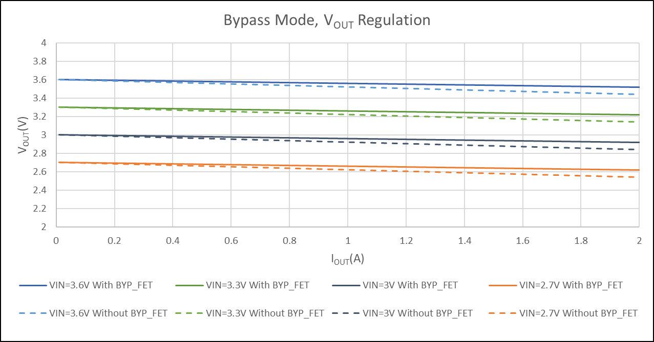
Figure 3. Output Voltage Comparison
1.3 Efficiency Close to 100%
By integrating the bypass switch, efficiency is improved from the typical 97% to 98% to nearly 100%, reducing power losses and minimizing heat dissipation.
Figure 4 compares the efficiency of Boost topology with and without a bypass switch. The solid line represents the efficiency with the bypass switch, highlighting that the Boost topology with a bypass switch is significantly more efficient than one without it.
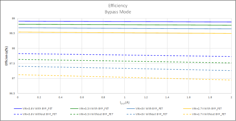
Figure 4. Efficiency Comparison
2 Product Key Features
The RT4803B operates within a voltage range of 1.8V to 5V, with an output voltage range of 2.85V to 4.4V. It offers 32 selectable output voltage levels, which can be chosen via the I2C communication interface, providing users with high flexibility. The RT4803B is packaged in a WL-CSP-16B 1.67x1.67 (BSC), making it ideal for miniaturized applications.
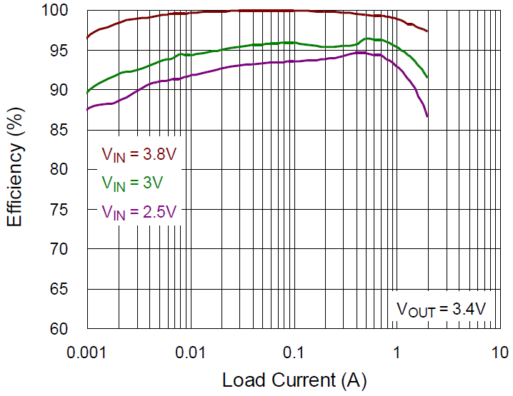
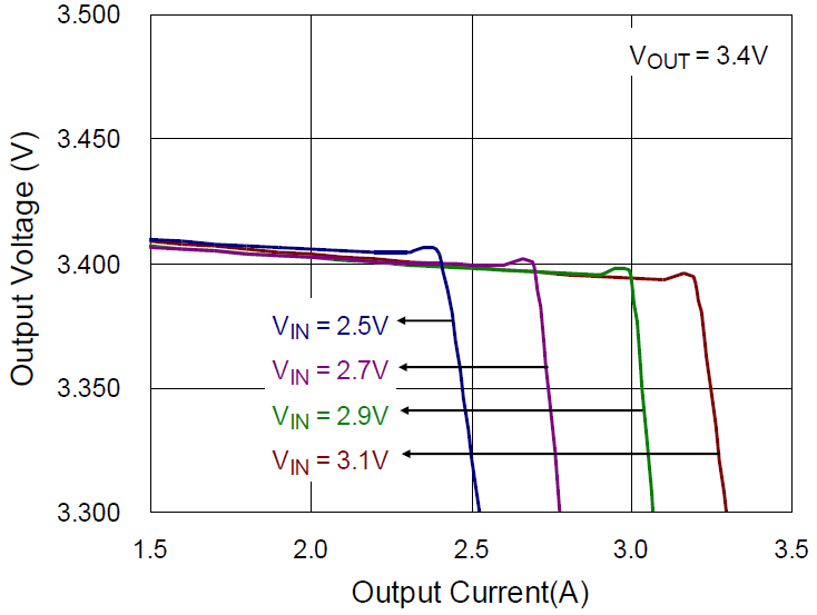
Below are the measurement data for the RT4803B, including efficiency and output voltage under different output current/input voltage.
|
|
|
|
Figure 5. Efficiency vs. Load Current
|
Figure 6. Output Voltage vs. Output Current
|
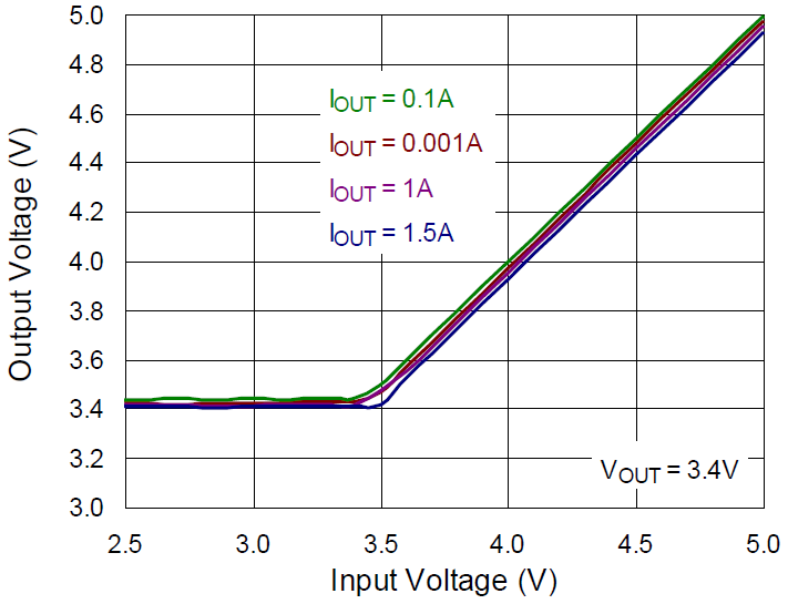
Figure 7. Output Voltage vs. Input Voltage
3 Design Example
Si-Anode battery known for their high capacity and low operating voltage characteristics, are becoming increasingly popular in mobile applications. As the operating voltage of Li-Ion battery decreases, a boost converter is required in the battery backend (system front-end) to supply power to the system. The RT4803B, with an operating voltage range of 1.8V to 5V, is highly suitable for Si-Anode battery-powered devices.
In certain applications, such as 2G PA, where precise output voltage regulation from the boost converter is not a strict requirement and only needs to be above the minimum operating voltage, the RT4803B with its bypass MOSFET offers a significant efficiency advantage. With only the conduction losses of the bypass switch (BYP_FET) and no inductor DCR losses, the efficiency in bypass mode approaches 100%, significantly enhancing battery utilization. Additionally, the RT4803B features a variety of protection functions, ensuring stable and efficient power management under various operating conditions. This makes it an ideal choice for power management in mobile and wearable devices.
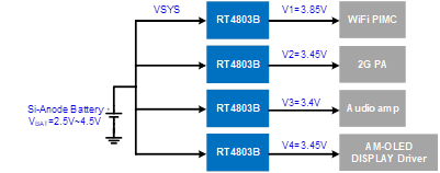
Figure 8. Mobile Device Design Example
Note: The above application circuit diagrams are for reference only. Actual products should be evaluated and adjusted according to your specific application requirements. For assistance, please contact our regional office.
To stay informed with more information about our products, please subscribe to our newsletter.